Did you already confirm that there is no problem with the switch reading code? A simple test would be to send a few hardcoded test bytes for simulated switch positions.
Have you tried different (slower) SPI speeds?
Do post the code if you can.
/Lars
Did you already confirm that there is no problem with the switch reading code? A simple test would be to send a few hardcoded test bytes for simulated switch positions.
Have you tried different (slower) SPI speeds?
Do post the code if you can.
/Lars
I am sure that the switch reading routine is working OK because when I single step thru the code and look at the values in via the JTAG and AVRStudio, they are correct. Further, when I single step, I get the correct switch codes at the receiver. I have also inserted as much as a one second delay for each trip thru the main loop, but it does not fix the problem.
Here’s the code.
/*

Handheld RF Robot Controller by Jim Lake 2006
Some of this software (the really clever stuff) was lifted from Lars Johnsson and is
subject to the following:
 * ----------------------------------------------------------------------------
 * "THE BEER-WARE LICENSE" (Revision 42):
 * Lars Jonsson (User name Lajon at www.avrfreaks.net) wrote this file.
 * As long as you retain this notice you can do whatever you want with this
 * stuff. If we meet some day, and you think this stuff is worth it, you can
 * buy me a beer in return.   Lars Jonsson
 * ----------------------------------------------------------------------------
 *
 The configuration of the nRF2401 is done using consants set out in trf24g_config.h
 config.h contains additional operational parameters. trf24g.h containes the function declarations

 Revision History:

 8/7/2006   1.0  Does not support USART, transmits the same 8 bit word via SPI.


 */
#include <stdio.h>
#include <stdlib.h>
#include <string.h>
#include <stdbool.h>
#include <avr/io.h>
#include <avr/signal.h>
#include <avr/interrupt.h>
#include "config.h"
#include <avr/delay.h>
#include "trf24g_config.h"
#include "trf24g.h"
#include "util.h"


#define TRF24G_START_CONFIG() TRF24G_CONTROL_PORT |= TRF24G_CS_MASK; _delay_us(5)
#define TRF24G_END_CONFIG()   TRF24G_CONTROL_PORT &= (uint8_t)~TRF24G_CS_MASK;

#define TRF24G_ACTIVE()   TRF24G_CONTROL_PORT |= TRF24G_CE_MASK; _delay_us(5)
#define TRF24G_INACTIVE() TRF24G_CONTROL_PORT &= ~TRF24G_CE_MASK;

#define SetBit(sfr, bit) ((sfr) |= (1 << (bit)))
#define ClearBit(sfr, bit) ((sfr) &= ~(1 << (bit)))


//_delay_us(10);  //slow things down


static uint8_t trf24gConfig[15] = {
   /*  0 */ TRF24G_PAYLOAD_SIZE * 8,   // DATA2_W
   /*  1 */ TRF24G_PAYLOAD_SIZE * 8,   // DATA1_W
   /*  2 */ 0,0,0,0,0,               // ADDR2 not used
   /*  7 */ TRF24G_ADDR1,            // ADDR1
   /* 12 */ ((TRF24G_ADDR_SIZE * 8) << 2) |
            ((TRF24G_CRC_SIZE == 0) ? 0b00 : ((TRF24G_CRC_SIZE == 1) ? 0b01 : 0b11)),
   /* 13 */ (0 << 7) |               // RX2 active or not (not for now)
          (1 << 6) |             // Shockburst (always)
          (TRF24G_1MBPS << 5) |      // Speed
          (0b011 << 2) |            // 16MHz always
          0b11,                       // Full power always
   /* 14 */ (TRF24G_CHANNEL << 1) | TRF24G_RX
 };
 #define ADDR1 7

int main (void){

	trf24gInit();
	while(1) {
		char buffer[TRF24G_PAYLOAD_SIZE];

		unsigned char Key;
		Key= KeyScan(); 	//scan the keys and returns: Key= an ASCII value for the key pressed
		/*
		while(KeyScan == 0xFF);
			ClearBit(PORTD, PD5);	//loops and makes the piezo buzz as long as two keys are pressed(this is a setbit for the buzzer)
	   }
	    SetBit(PORTD, PD5);    //Stop the buzzer
		*/

		buffer[0] = Assemble_Data(Key);
		trf24gSend(buffer);
		_delay_ms((TRF24G_TIME_ON_AIR + 999) / 1000); /* round up to ms */

   }
	return 0;
}


static inline uint8_t spiSend(uint8_t d)
{
   SPDR = d;	//Load a byte into the SPI data buffer for transfer

   while(!(SPSR & (1<<SPIF)))		//wait until transmission is complete
      ;
   return SPDR;
}

void trf24gInit(void)
{
   uint8_t i;

   // DDR for trf24g control, CS and CE are outputs
   TRF24G_CONTROL_DDR |= TRF24G_CS_MASK|TRF24G_CE_MASK;
    // DDR for SPI, MOSI and SCK are outputs
   TRF24G_SPI_DDR |= TRF24G_SPI_MOSI_MASK|TRF24G_SPI_SCK_MASK;
   SetBit(PORTB, PB4); //drive SS high
   // SPI master, trailing edge setup
   SPCR = (1<<SPE)|(1<<MSTR)|(1<<SPR0); // /8 clock (8Mhz/8 = 1Mhz)
    SPSR |= (1<<SPI2X);
   //SPCR = (1<<SPE)|(1<<MSTR)|(0<<SPR0); // /4 clock (works also)
   _delay_ms(3);   // >3ms startup
    TRF24G_START_CONFIG();		//take CS high
   for(i = 0; i < sizeof(trf24gConfig); i++) {		//send the configuration word to the SPI
      spiSend(trf24gConfig[i]);
   }
   TRF24G_END_CONFIG();     //take CS low
   //ClearBit(DDRB, DDB5);    //Make MOSI an input to eliminate conflict with MISO
#if TRF24G_RX		//if we are a receiver, send CE high to make the transiever poll the air
   TRF24G_ACTIVE();
#endif
}

void trf24gSend(void *p)
{
   uint8_t n = TRF24G_ADDR_SIZE;
   uint8_t *buf = (uint8_t*)p;  //pointer to the beginning of the data array to be sent
   uint8_t *a = trf24gConfig + ADDR1 + 5 - TRF24G_ADDR_SIZE;   //pointer to the address section of the config word

   TRF24G_ACTIVE();   //CE high
   do {
      spiSend(*a++);
   } while(--n);
   n = TRF24G_PAYLOAD_SIZE;
   do {
      spiSend(*buf++);  //this sends the first element in the array buffer[0] first
   } while(--n);
   TRF24G_INACTIVE();    //CE low
}


/*
void trf24gReconfigure(uint8_t channel, bool rx)
{
   uint8_t cfg = channel << 1;
   cfg |= rx;

   TRF24G_INACTIVE();
   TRF24G_START_CONFIG();
   spiSend(cfg);
   TRF24G_END_CONFIG();
   if (rx) {
      TRF24G_ACTIVE();
   }
}


bool trf24gReceive(void *p)
{
	//redefine MOSI as an input to accept data from the DATA pin
	//DDRB |= (0 << DDB5);

   uint8_t dr = TRF24G_DR1_PIN & TRF24G_DR1_MASK;
   if (dr) {
      uint8_t n = TRF24G_PAYLOAD_SIZE;
      uint8_t *buf = (uint8_t*)p;  // *buf points to the first element in the array
      do {
         *buf++ = spiSend(0);    //fill up the array by incrementing the buffer and swapping bits with the spi
      } while(--n);
   }
   return dr;
}
*/

/*

Keyscan     2006 Jim Lake

Called By: Main()
Ruturns: unsigned char Key an ASCII char representing which switch is pressed, no press returns zero

This routine will scan a 2x4 switch matrix wired as follows:

PORT		        key		        row

PA0	________|select_____|up          1
PA1	________|down_______|right       2
PA2	________|left_______|sw1         3
PA3	________|sw2________|sw3         4
			|			|
PA4_________|			|
PA5_____________________|

The circuit contemplates an ITT  TPA series nav switch and 3 button switches for a total of 8 bits
PA0-PA3 are outputs in sequence, PA4 and PA5 are inputs with pull ups enabled

The code uses a macro supplied by the avr-gcc compiler:
*		bit_is_clear(sfr, bit) -- this returns:
*			true if the given "bit" in the specified "sfr" is clear (0), or
*			false if the bit is set (1).
*		(There is also the opposite macro: bit_is_set(sfr, bit).)
*
*/

unsigned char KeyScan(void){

	DDRA = 0x0F;          //  0000  1111   PA0-PA3 are outputs, PA4 and PA5 are inputs
	PORTA = 0x30;        //   0011  0000   pull ups on PA4 and PA5
	unsigned char NumKey;
	unsigned char Key;
	NumKey = 0;	//No keys pressed
	Key = 0; 	//defaults to zero

	//***************ROW1*******************************
	DDRA = 0x01;	//select row 1 (Up and Select)    0000 0001
	if(bit_is_clear(PINA, PINA4)){
		Key = 'u';	//Up is pressed
		NumKey++;
	}
	if(bit_is_clear(PINA, PINA5)){
		Key = 's';	//Select is pressed
		NumKey++;
	}
	//***************ROW2********************************
	DDRA = 0x02;	//select row 2 (Right and Down)   0000 0010
	if(bit_is_clear(PINA, PINA4)){
		Key = 'r';	//Right is pressed
		NumKey++;
	}
	if(bit_is_clear(PINA, PINA5)){
		Key = 'd';	//Down is pressed
		NumKey++;
	}
	//****************ROW3******************************
	DDRA = 0x04;	//select row 1 (Sw1 and Left)   0000 0100
	if(bit_is_clear(PINA, PINA4)){
		Key = '1';	//Switch 1 is pressed
		NumKey++;
	}
	if(bit_is_clear(PINA, PINA5)){
		Key = 'l';	//Left is pressed
		NumKey++;
	}
	//****************ROW4*******************************
	DDRA = 0x08;	//select row 4 (Switch 2 and Switch 3)  0000 1000
	if(bit_is_clear(PINA, PINA4)){
		Key = '2';	//Switch 2 is pressed
		NumKey++;
	}
	if(bit_is_clear(PINA, PINA5)){
		Key = '3';	//Switch 3 is pressed
		NumKey++;
	}
	//***************************************************
	if (NumKey > 1){
		Key = 0xFF;		//Multiple key pressed error
	}

	DDRA = 0x0F;	//All rows are outputs, columns are inputs

	return Key;
}

/*
void USART_Init(unsigned int baud)		// Initialize the USART for coms to a terminal

{

	// set the baud rate to 19.2 kbps

	UBRRH = (unsigned char) (baud >> 8);

	UBRRL = (unsigned char) baud; //this is decimal 25 see page 167 data sheet

	// Enable RX and TX

	UCSRB = (1<<RXEN) | (1<< TXEN);

	// set the frame format to 8 data bits, 2 stop bits, no parity

	UCSRC = (1<<URSEL) |(1<<USBS)  | (3<<UCSZ0);

}


void USART_Transmit(unsigned int data)
{
	// Wait for an empty transmit buffer

	while (!(UCSRA & (1<<UDRE)));

	//Place data in the buffer and transmit it

	UDR = data;

}

*/
*
Assemble_Data Jim Lake  2006

Called From: Main()
Returns: char databyte
Assembles a data word representing the switch setting scanned in KeyScan(). KeyScan returns one of the ASCII values below:
'r' = right
'l'= left
'u'= up
'd'= down
's'= select
'1'= switch1
'2'= switch2
'3'= switch3

The dataword is a follows:

bit7		bit6		bit5		bit4		bit3		bit2		bit1		bit0

SW3			SW2			SW1			select		right		left		down		up

*/
char Assemble_Data(unsigned char Key){
	unsigned char databyte = 0;
	switch(Key){
	case 'u': databyte = 0x01; return databyte;
	case 'd': databyte = 0x02; return databyte;
	case 'l': databyte = 0x04; return databyte;
	case 'r': databyte = 0x08; return databyte;
	case 's': databyte = 0x10; return databyte;
	case '1': databyte = 0x20; return databyte;
	case '2': databyte = 0x40; return databyte;
	case '3': databyte = 0x80; return databyte;
	default:                   return databyte;
	}
}
Its is a puzzle.
Thanks, Jim Lake
Well single stepping is not a good test of code that can depend on timing. In your scan function I think there might be a problem if the output can't pull down the current row fast enough. Try with a delay (after all 4 DDR settings):I am sure that the switch reading routine is working OK because when I single step thru the code and look at the values in via the JTAG and AVRStudio, they are correct.
   DDRA = 0x01;   //select row 1 (Up and Select)    0000 0001
   _delay_us(8); // wait for stable output (more or less might be needed)
You could test just that key scanning with output on the USART just to be sure. Same for the RF part (constant test values - just verify they arrive ok).
/Lars
You DO need to delay when scanning codes. It takes 1 or 2 cpu clocks to have the input pin settle when it changes state. I had this problem when scanning a keypad too. The results of a scan showed me what I expected to see from the PREVIOUS scan!
Insert three nop(); instructions between setting the output pin(s) and reading the input pins.
That solved the problem for me.
-Tony
Thanks guys,
That makes sense and I will try it.
Just a follow up on the above. I added the nop’s and the problem disappeared. Thanks for the help. The little critter works perfectly now.
Hi you guys,
Sorry to bother you with such silly questions, but here goes nothing.
I own a couple of TRW-24g (or RF-24g) bought from sparkfun.
My goal is to build a serial2RF transmitter and a RF2serial receiver.
I want to use AtMega8 to do so.
Can anyone help me with a schematics for the PCB or even just an explanation for what I must do.
I know the TRW-24g (or again, the RF-24g) works with 3.3v but the AtMega8 uses 5v. what do I do in order to use the AtMega8 In spite of it.
Tal.
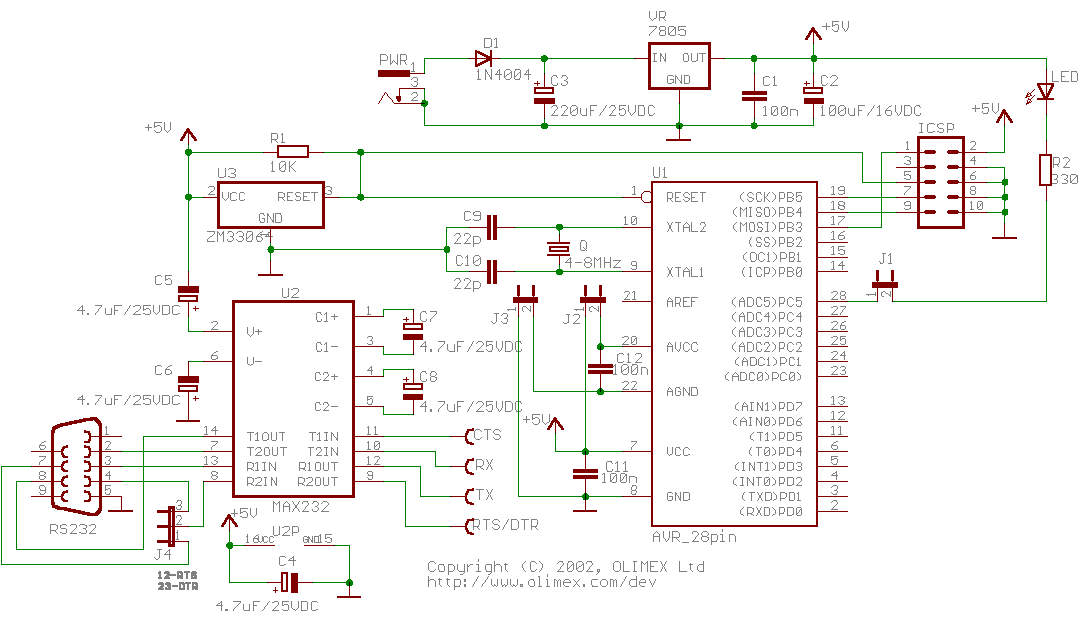
Well the SPI connections for the RF-24g are shown in the document I refer to in the first post in this thread. Apart from that is should be no more than the RS-232 (if that is the serial interface you want) for which you will need a transciever. Have a look at the development boards schematics e.g.
http://www.sparkfun.com/datasheets/AVR/avr-p28b-sch.gif
(You can probably skip the reset controller in that design, just pull up reset with 4K7 or so).
It would simplify things if you you could run the AVR at 3.3V also. So a ATMega8L or one of the newer ATMega48/88/168. You will want to run it with a crystal (not the internal clock), 7.3728 MHz would be good for supporting common serial speeds.
/Lars
Ok, most of the work done. at least, I’ve thought.
I want two computer to communicate serially over RF (using the TRW-24g).
I’ve built a PCB that uses Atmega88 which connect through max3232 to RS232 (for USART) on one hand and to the TRW-24g on the other (using SPI).
The USART working great.
I’m NOT using external clock. (will it affect only the USART, of the SPI too?)
I’m working for the serial with baud rate 4800.
the UBRR is 12.
I’ve set the F_CPU to 8E6.
what are all those speeds?
what does the speed (16Mhz on Lars’s example) do?
What does it has to do with the clock speed (8Mhz)?
Can you please help me to understand all the speeds/baud rates.
You can assume, that I’ve built the PCB right, and all the MASKs/PORTs fits.
This is my code:
/*
 * ----------------------------------------------------------------------------
 * "THE BEER-WARE LICENSE" (Revision 42):
 * Lars Jonsson (User name Lajon at www.avrfreaks.net) wrote this file.
 * As long as you retain this notice you can do whatever you want with this
 * stuff. If we meet some day, and you think this stuff is worth it, you can
 * buy me a beer in return.   Lars Jonsson
 * ----------------------------------------------------------------------------
 *
 */
#include <stdio.h>
#include <stdlib.h>
#include <string.h>
#include <stdbool.h>
#include <avr/io.h>
#include <avr/signal.h>
#include <avr/interrupt.h>
#include "config.h"
#include <avr/delay.h>
#include "trf24g_config.h"
#include "trf24g.h"


#define TRF24G_START_CONFIG() TRF24G_CSCE_PORT |= TRF24G_CS_MASK; _delay_us(5)
#define TRF24G_END_CONFIG()   TRF24G_CSCE_PORT &= (uint8_t)~TRF24G_CS_MASK;

#define TRF24G_ACTIVE()   TRF24G_CSCE_PORT |= TRF24G_CE_MASK; _delay_us(5)
#define TRF24G_INACTIVE() TRF24G_CSCE_PORT &= ~TRF24G_CE_MASK;

static uint8_t trf24gConfig[15] = {
   /*  0 */ TRF24G_PAYLOAD_SIZE * 8,   // DATA2_W
   /*  1 */ TRF24G_PAYLOAD_SIZE * 8,   // DATA1_W
   /*  2 */ 0,0,0,0,0,               // ADDR2 not used
   /*  7 */ TRF24G_ADDR1,            // ADDR1
   /* 12 */ ((TRF24G_ADDR_SIZE * 8) << 2) |
            ((TRF24G_CRC_SIZE == 0) ? 0b00 : ((TRF24G_CRC_SIZE == 1) ? 0b01 : 0b11)),
   /* 13 */ (0 << 7) |               // RX2 active or not (not for now)
          (1 << 6) |             // Shockburst (always)
          (TRF24G_1MBPS << 5) |      // Speed
          (0b011 << 2) |            // 16MHz always
          0b11,                       // Full power always
   /* 14 */ (TRF24G_CHANNEL << 1) | TRF24G_RX
 };
 #define ADDR1 7

static inline uint8_t spiSend(uint8_t d)
{
   SPDR = d;
   while(!(SPSR & (1<<SPIF)))
      ;
   return SPDR;
}

void trf24gInit(void)
{
   uint8_t i;

   // DDR for trf24g control, CS and CE are outputs
   TRF24G_CSCE_DDR |= TRF24G_CS_MASK|TRF24G_CE_MASK; //@tal
    // DDR for SPI, MOSI and SCK are outputs
   TRF24G_SPI_DDR |= TRF24G_SPI_MOSI_MASK|TRF24G_SPI_SCK_MASK;
   TRF24G_SPI_SS_PORT |= TRF24G_SPI_SS_MASK; //drive SS high //@tal
   // SPI master, trailing edge setup
   SPCR = (1<<SPE)|(1<<MSTR)|(1<<SPR0); // /8 clock (8Mhz/8 = 1Mhz)
    SPSR |= (1<<SPI2X);
   //SPCR = (1<<SPE)|(1<<MSTR)|(0<<SPR0); // /4 clock (works also)
   _delay_ms(3);
   // >3ms startup
   TRF24G_START_CONFIG();
   for(i = 0; i < sizeof(trf24gConfig); i++) { //send the configuration word to the SPI
      spiSend(trf24gConfig[i]);
   }
   TRF24G_END_CONFIG();
#if TRF24G_RX
   TRF24G_ACTIVE();
#endif
}

void trf24gReconfigure(uint8_t channel, bool rx)
{
   uint8_t cfg = channel << 1;
   cfg |= rx;

   TRF24G_INACTIVE();
   TRF24G_START_CONFIG();
   spiSend(cfg);
   TRF24G_END_CONFIG();
   if (rx) {
      TRF24G_ACTIVE();
   }
}

bool trf24gReceive(void *p)
{
   uint8_t dr = TRF24G_DR1_PIN & TRF24G_DR1_MASK;
   if (dr) {
      uint8_t n = TRF24G_PAYLOAD_SIZE;
      uint8_t *buf = (uint8_t*)p;
      do {
         *buf++ = spiSend(0);
      } while(--n);
   }
   return dr;
}

void trf24gSend(void *p)
{
   uint8_t n = TRF24G_ADDR_SIZE;
   uint8_t *buf = (uint8_t*)p;
   uint8_t *a = trf24gConfig + ADDR1 + 5 - TRF24G_ADDR_SIZE;

   TRF24G_ACTIVE();
   do {
      spiSend(*a++);
   } while(--n);
   n = TRF24G_PAYLOAD_SIZE;
   do {
      spiSend(*buf++);
   } while(--n);
   TRF24G_INACTIVE();
}


//#####################################################################
//#######################         USART         #######################
//#####################################################################

void usart_putc(unsigned int input) {
   // wait until UDR ready
	while(!(UCSR0A & (1 << UDRE0)));
	UDR0 = input;    // send USART
}


void setBoudRateByMethod()
{

		UBRR0H = 0;
		UBRR0L = 12;


}

void usart_init()
{
	// init the USART (Universal Sync and ASync Receiver and Transmiter) bits

	// there 3 groups of control status bits (UVSR[A-C])
	UCSR0A = (1<<RXC0); // clear the Receive Bit
	UCSR0B = (1<<RXEN0) | (1<<TXEN0) | (1<<RXCIE0); // enable Receive Rx;enable Transmit Tx;Enable Rx Interrupt
	UCSR0C = (3<<UCSZ00) | (1<<UMSEL01) | (1<<USBS0); // 8 dataBits, No parity, and 2 stopBits

	setBoudRateByMethod();
}


SIGNAL(SIG_USART_RECV)
{
	unsigned int input;
	while (!(UCSR0A & (1 << RXC0)));
	input=UDR0; // read an int from the serial port

	PORTC |= (1 << PC4); //@TODO - remove, just for debug

	char buffer[TRF24G_PAYLOAD_SIZE];
	buffer[0] = input;
	trf24gSend(buffer);
	_delay_ms((TRF24G_TIME_ON_AIR + 999) / 1000); /* round up to ms */
	usart_putc(input + 1); // for debug, the sender will return it to the terminal
}


//#####################################################################
//#######################         main          #######################
//#####################################################################


int main(void)
{

	trf24gInit();
	usart_init(); // init USART

	PORTC &= (0 << PC5); //@TODO - remove, just for debug
	PORTC &= (0 << PC4); //@TODO - remove, just for debug

	// ####################
	// #### The SENDER ####
	// ####################

    if (TRF24G_RX == 0)
	{
		PORTC |= (1 << PC5); //@TODO - remove, just for debug
		sei();   // enable interrupts
		while(1)
		{

		}
	} else
	// ######################
	// #### The RECEIVER ####
	// ######################
	{
		PORTC |= (1 << PC4); //@TODO - remove, just for debug
		while(1)
		{
			char buffer[TRF24G_PAYLOAD_SIZE];
			if (trf24gReceive(buffer))
			{
				usart_putc(buffer);
			}
		}
	}

	return(0);
}
UBRR0L = 12;
If this gives you 4800 baud then your AVR is running at 1Mhz (look in the Table 81. Examples of UBRRn Settings for Commonly Used Oscillator Frequencies). A new mega 88 runs at 1Mhz, you need to unprogram the CKDIV8 fuse to have it run at 8Mhz. And yes, the SPI should be ok with the internal RC Oscillator.
``` (0b011 << 2) | // 16MHz always ``` This is just configuration for the TRW-24g (it has a 16MHz crystal).what does the speed (16Mhz on Lars’s example) do?
Nothing.What does it has to do with the clock speed (8Mhz)?
Maybe you should start with some simpler code, sending a constant character (so not using that interrupt in the first test). It is BTW usually not a good idea to have too much work done in an interrupt handler. You should probably just collect the characters in a buffer and send them from the main.
Also,
usart_putc(buffer);
I guess should be
usart_putc(buffer[0]);
/Lars
HI!
I am having some problems with my code for the trf24g and find it cind of difficult to debug internaly in the reciver. The sender sends one byte of data into the tranciver, but the DR1 pin on the reciver doesent go high at any time.
I would apriciate any help i can get.
RX code :
#include <mega16.h>
#include <stdio.h>
#include <delay.h>


#define CE PORTB.0
#define CS PORTB.1


//*******************************************************************************************
 // configuration word :  (15 bytes)


/*15*/    #define TRF24G_PAYLOAD_SIZE_1  1		// in bytes

/*14*/    #define TRF24G_PAYLOAD_SIZE_2  1		// in bytes

/*9-13*/  #define TRF24G_ADDR_2  0,0,0,0,0 		// 5 bytes (not in use)

/*4-8*/   #define TRF24G_ADDR_1  0,0,0,0,0xAA       // 5 bytes

/*3*/  	  #define TRF24G_ADDR_SIZE  1               // in bytes
	      #define TRF24G_CRC_SIZE 0b01          // 8 bit CRC enabled

/*2*/	  #define TRF24G_RX2_EN 0                   // RX2 dissabled
	      #define TRF24G_SHOCK_EN 1             // shock burst enabled
	      #define TRF24G_DATARATE 0             // 0 for 250kbs or 1 for 1mbs
	      #define TRF24G_XTAL_FREQ 0b011        // 16mhz inside unit
	      #define TRF24G_TX_PWR 0b11            // FULL power !!

/*1*/     #define TRF24G_CHANNEL 2		    // channel 2
	      #define TRF24G_RX 0                   // 0 for TX or 1 for RX


// end of config word.


//******************************************************************************************
// tabell for configurerings ordet.

static unsigned char trf24gConfig[15] =  {


/*15*/	  TRF24G_PAYLOAD_SIZE_2 * 8,            // DATA2_W in bits

/*14*/    TRF24G_PAYLOAD_SIZE_1 * 8,            // DATA1_W in bits

/*9-13*/  TRF24G_ADDR_2,                        // ADDR2 (not in use)

/*4-8*/   TRF24G_ADDR_1,                        // ADDR1

/*3*/     ((TRF24G_ADDR_SIZE * 8) << 2) | TRF24G_CRC_SIZE,

/*2*/     (TRF24G_RX2_EN << 7) |                // RX2 active?
          (TRF24G_SHOCK_EN << 6) |              // Shockburst?
          (TRF24G_DATARATE << 5) |              // Datarate
          (TRF24G_XTAL_FREQ << 2) |             // xtal frequency
           TRF24G_TX_PWR , 			            // Tx power

/*1*/     (TRF24G_CHANNEL << 1) | TRF24G_RX	// Channel and RX/TX select

};


//***************************************************************************************

void vent ()
 {
 delay_ms(5);
 }

//*********************************************************************************


void spiSend(unsigned char data)
{
   #asm("cli")  // disable interrupts
   SPDR = data;
   while(SPSR == 0x00)
   {
    //wait for sending to finish
   }
   #asm("sei")  // enable interrupts
}

//****************************************************************************************

void trf24gconfigure(unsigned char trf24gConfig[15]) {

   unsigned char i;


	delay_ms(3);      // 3ms startup

	CE = 0 ;
        vent() ;	  // enter config mode
	CS = 1 ;


   for(i = 0; i < sizeof(trf24gConfig); i++)
   {
      spiSend(trf24gConfig[i]);		// sending...
   }


	CS = 0 ;      // exit config mode
	vent() ;

#if TRF24G_RX
        CE = 1 ;      // activate RX
        vent() ;
#endif

}


//****************** RECIVING ***********************************************************


// External Interrupt 0 service routine   (interupts when data ready (DR =1) )
interrupt [EXT_INT0] void ext_int0_isr(void)
{
unsigned char data;
int i ;
unsigned char size = TRF24G_PAYLOAD_SIZE_1;
printf ("\n\r%d", 0x22 ) ;     // for debug

#asm("cli")    // disable interupt

printf ("\n\r%d", 0x21 ) ;            // for debug
   spiSend (0x00) ;			// sends 0, when finished SPI interrupts


 for(i = 0; i < size ; i++)
   {

     data = SPDR ;
     printf ("\n\r%d", 0x20 ) ;            // for debug
     printf ("\n\r%d", data ) ;
     spiSend (0x00) ;

   }
   vent() ;


  #asm("sei")     // enable interupt
}


//*****************************************************************************************************
void main(void)
{

PORTB=0x00;
DDRB=0xB3;

PORTD=0x00;
DDRD=0x02;

// SPI initialization
// SPI Type: Master
// SPI Clock Rate: 62,000 kHz
// SPI Clock Phase: Cycle Half
// SPI Clock Polarity: Low
// SPI Data Order: MSB First
SPCR=0x53;
SPSR=0x00;


//USART
UCSRA=0x00;
UCSRB=0x18;
UCSRC=0x86;
UBRRH=0x00;
UBRRL=0x33;


// External Interrupt(s) initialization
// INT0: On
// INT0 Mode: Rising Edge
// INT1: Off
// INT2: Off
GICR|=0x40;
MCUCR=0x03;
MCUCSR=0x00;
GIFR=0x40;


// Clear the SPI interrupt flag
#asm
    in   r30,spsr
    in   r30,spdr
#endasm

// Global enable interrupts
#asm("sei")


trf24gconfigure(trf24gConfig);		// configure RF24g


while (1)
{

//just let the interupt work(RX-mode)

}

}// main
TX code:
// transmitter code for RF 24g

#include <mega8.h>
#include <stdio.h>
#include <delay.h>


#define CE PORTB.6
#define CS PORTB.7


//*******************************************************************************************
 // configuration word :  (15 bytes)


/*15*/    #define TRF24G_PAYLOAD_SIZE_1  1		// in bytes

/*14*/    #define TRF24G_PAYLOAD_SIZE_2  1		// in bytes

/*9-13*/  #define TRF24G_ADDR_2  0,0,0,0,0 		// 5 bytes (not in use)

/*4-8*/   #define TRF24G_ADDR_1  0,0,0,0,0xAA   // 5 bytes

/*3*/  	  #define TRF24G_ADDR_SIZE  1           // in bytes
	      #define TRF24G_CRC_SIZE 0b01          // 8 bit CRC enabled

/*2*/	  #define TRF24G_RX2_EN 0               // RX2 dissabled
	      #define TRF24G_SHOCK_EN 1             // shock burst enabled
	      #define TRF24G_DATARATE 0             // 0 for 250kbs or 1 for 1mbs
	      #define TRF24G_XTAL_FREQ 0b011        // 16mhz inside unit
	      #define TRF24G_RX_PWR 0b11            // FULL power !!

/*1*/     #define TRF24G_CHANNEL 2			    // channel 2
	      #define TRF24G_RX 0                   // 0 for TX or 1 for RX


// end of config word.


//******************************************************************************************


unsigned char trf24gConfig[15] =  {   // tabell for configurerings ordet.


/*15*/	  TRF24G_PAYLOAD_SIZE_2 * 8,            // DATA2_W in bits

/*14*/    TRF24G_PAYLOAD_SIZE_1 * 8,            // DATA1_W in bits

/*9-13*/  TRF24G_ADDR_2,                        // ADDR2 (not in use)

/*4-8*/   TRF24G_ADDR_1,                        // ADDR1

/*3*/     ((TRF24G_ADDR_SIZE * 8) << 2) | TRF24G_CRC_SIZE,

/*2*/     (TRF24G_RX2_EN << 7) |                // RX2 active?
          (TRF24G_SHOCK_EN << 6) |              // Shockburst?
          (TRF24G_DATARATE << 5) |              // Datarate
          (TRF24G_XTAL_FREQ << 2) |             // xtal frequency
           TRF24G_RX_PWR , 			            // Tx power

/*1*/     (TRF24G_CHANNEL << 1) | TRF24G_RX	// Channel and RX/TX select

};


//***************************************************************************************


void vent ()
 {
 delay_us(5);
 }

//*********************************************************************************

void spiSend(unsigned char data)
{
   SPDR = data;
   while(SPSR == 0x00)
   {
    //wait for sending to finish
   }

}


//****************************************************************************************
void trf24gconfigure(unsigned char trf24gConfig[15])
{
   unsigned char i;


	delay_ms(3);      // 3ms startup

	CE = 0 ;
        vent() ;	  // enter config mode
	CS = 1 ;


   for(i = 0; i < sizeof(trf24gConfig); i++)
   {
      spiSend(trf24gConfig[i]);		// sending...
   }


	CS = 0 ;      // exit config mode
	vent() ;

#if TRF24G_RX
        CE = 1 ;      // activate RX
#endif

}

//******************************************************************************************


void trf24gSend(char data)    // for 1 byte data and address
{

   unsigned char addr = 0xAA;

  	CE = 1 ;
        vent() ;	 // enter sending mode
	CS = 0 ;

     spiSend(addr);     //adress
     vent () ;
     spiSend(data);     // DATA

     vent () ;

     CE = 0 ;         //back to standby


}


//*****************************************************************************************************
void main(void)
{

PORTB=0x00;
DDRB=0xFF;

PORTC=0x00;
DDRC=0x00;


// SPI initialization
// SPI Type: Master
// SPI Clock Rate: 62,000 kHz
// SPI Clock Phase: Cycle Half
// SPI Clock Polarity: Low
// SPI Data Order: MSB First
SPCR=0x53;
SPSR=0x00;


//USART
UCSRA=0x00;
UCSRB=0x18;
UCSRC=0x86;
UBRRH=0x00;
UBRRL=0x33;


trf24gconfigure(trf24gConfig);		// configure RF24g


while (1)
{

trf24gSend(0x24) ;
delay_ms (1000) ;

}


}// main
You have
#define TRF24G_RX 0 // 0 for TX or 1 for RX
in the rx code, this should be 1 for rx.
/Lars
This topic is a little old, but I’m wondering if anyone is still in touch with it?
Thanks
Monte
Well as you notice I don’t read here every day but if you have a question go ahead and ask.
/Lars
Ok reading the code a bit closer i saw what you did. just sending the destination adress byte for byte and then payload