Hello all! I’m new to these forums and I’m also relatively new to electronics. I want to share a project I’ve been working on for the past few months.
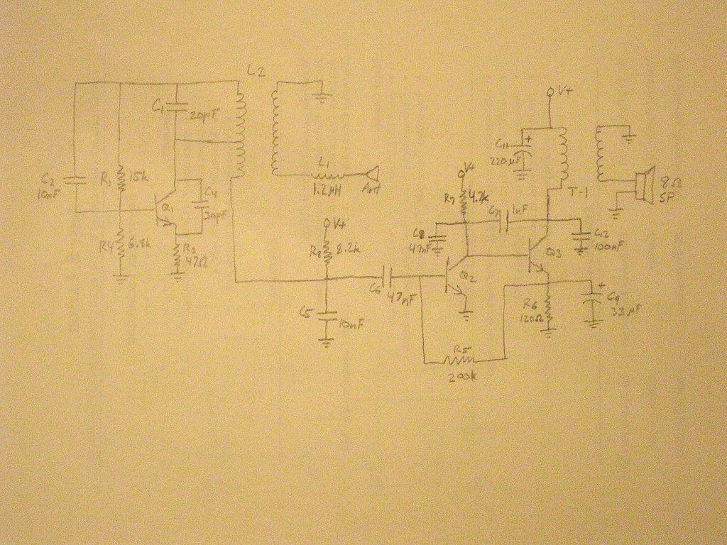
I have been reverse engineering a pair of walkie talkies that I’ve had since I was a kid. I finally have a circuit diagram (that part took the longest) but there is a “mystery component” that I need help indentifying, namely L2. I am not familiar with the layout of this type of FM transciever so if there is something that ‘clicks’ and makes sense to you please post! I would be very interested in what any information that would shed some light on the how and why of this circuit.
Here’s what I know:
-
Powered with a 9 volt battery
-
Classified by the FCC as DXC Part 15 Low Power Transceiver, Rx Certified
-
FM modulated
-
Upper frequency listed as 49.90000000 Mhz
-
Lower frequency listed as 49.82000000 Mhz
-
Uses the speaker as a microphone when transmitting.
-
Q1 is a C3192 transistor (High Frequency) http://pdf1.alldatasheet.com/datasheet- … C3192.html
-
Q2 and Q3 are C3198 transistors (general purpose) http://pdf1.alldatasheet.com/datasheet- … C3198.html
-
Q1 has a ferrite bead on its emitter
-
L2 is variable but comes glued in place from the factory
-
L2 seems to have the configuration of a centertapped transformer but I’ve only been able to test this with a multimeter since I don’t have a function generator. I did cut the traces to remove it from the circuit before measuring.
Pics!
 http://farm6.static.flickr.com/5121/533 … e13c3e.jpg
The hardware!
 http://farm6.static.flickr.com/5009/533 … 371c29.jpg
 <LINK_TEXT text=“http://farm6.static.flickr.com/5209/533 … b573_z.jpg”>http://farm6.static.flickr.com/5209/5335981281_182af8b573_z.jpg</LINK_TEXT>
[fm_circuit2 by [East_India_Tea, on Flickr
The 12 pin component is the push to talk switch and the middle unlabeled component is the On-Off switch
 http://farm6.static.flickr.com/5009/533 … f59b1f.jpg
L2 is that strange white and black component on the left.
 http://farm6.static.flickr.com/5087/533 … 34fc75.jpg
Another view of L2
 <LINK_TEXT text=“http://farm6.static.flickr.com/5248/533 … a861_b.jpg”>http://farm6.static.flickr.com/5248/5335933741_5388dea861_b.jpg</LINK_TEXT>
[Transmitting Circuit Diagram by [East_India_Tea, on Flickr
Transmitting
 <LINK_TEXT text=“http://farm6.static.flickr.com/5045/533 … 981a_b.jpg”>http://farm6.static.flickr.com/5045/5335933727_8b05e8981a_b.jpg</LINK_TEXT>
[Receiving Circuit Diagram by [East_India_Tea, on Flickr
Receiving
Eventually I hope to build a new pair from these schematics if I can understand this circuit.
Thanks! :)](About East_India_Tea | Flickr)](Receiving Circuit Diagram | After much work, an actual circu… | Flickr)](Receiving Circuit Diagram | After much work, an actual circu… | Flickr)](About East_India_Tea | Flickr)](Transmitting Circuit Diagram | This is the schematic for tra… | Flickr)](Transmitting Circuit Diagram | This is the schematic for tra… | Flickr)](About East_India_Tea | Flickr)](fm_circuit2 | Circuit board after all components are labeled… | East_India_Tea | Flickr)](fm_circuit2 | Circuit board after all components are labeled… | East_India_Tea | Flickr)