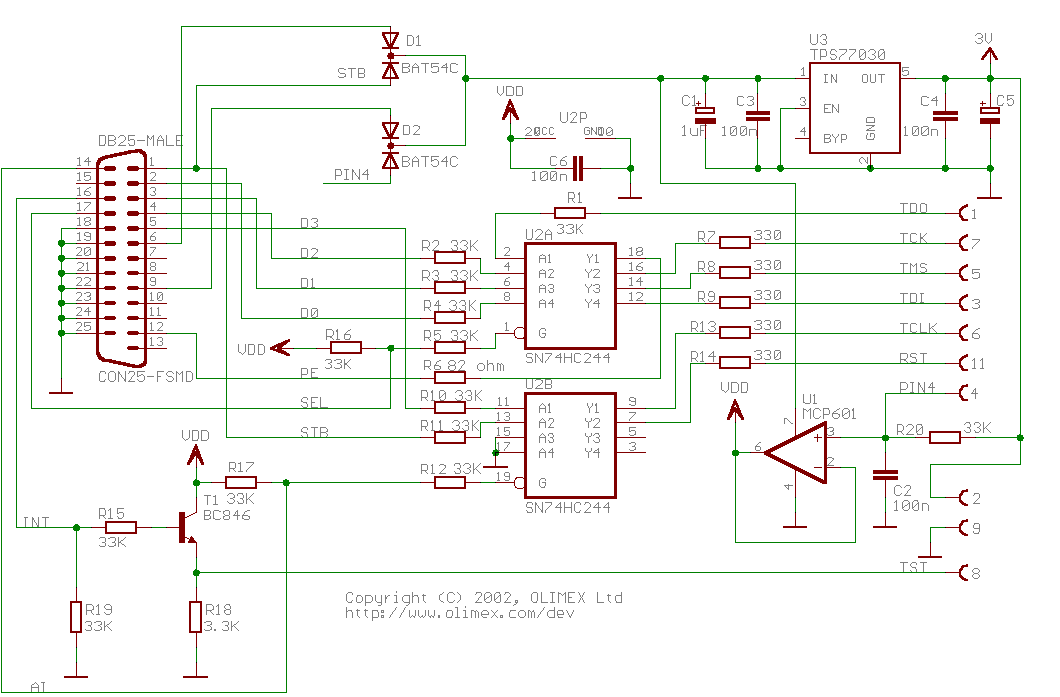
Can somebody tell me what is the d1 adn d2 the pin 4 where does it go rom d2 and the pins form u2d where there are connected? because in the schematic is superimposed.
D1 and D2 are dual diodes with a common cathode. They are used to route power to the JTAG. The anode of one of the diodes in D2 connects to pin 4 of the JTAG connector.
I’m not sure what you mean by “u2d”. If you are talking about U2P, that is the power connection for the SN74HC244 and the schematic is showing you that pin 20 should be connected to VCC and pin 10 should be connected to GND and that a 100nF bypass capacitor is connected between VCC and GND.
gm:
D1 and D2 are dual diodes with a common cathode. They are used to route power to the JTAG. The anode of one of the diodes in D2 connects to pin 4 of the JTAG connector.
I’m not sure what you mean by “u2d”. If you are talking about U2P, that is the power connection for the SN74HC244 and the schematic is showing you that pin 20 should be connected to VCC and pin 10 should be connected to GND and that a 100nF bypass capacitor is connected between VCC and GND.
