LPc2138

I believe I have connected the vss pins to the VSS battery and VDD on VDD battery…

These are connected to the VDD pinhead where the Polymer Lithium battery will be connected…

VDD3-1

VDD3-2

VDD3-3

VDDA3

VBAT

And these are the VSS pins where the VSS pinhead of the battery will be connected…

VSS(pin 6)

VSS(pin 18)

VSS(pin 25)

VSS(pin 42)

VSS(pin 50)

VSSA

I still haven’t connected VREF anywhere because thats what you told me…

New schematic http://www.megaupload.com/?d=VMLRWL57

As you’ve been told repeatedly, give up this project and try something much simpler.

leon_heller:
As you’ve been told repeatedly, give up this project and try something much simpler.

Not going to…

Well The vdd and vss pins are connected, what did you meant when you said they were connected wrongly?

The pins were just connected to the capacitors, not to the supply and ground.

Post the schematic here, no none is going to download it from another site.

Now that it gets better, what can I do?

The Vdd connections are still wrong!

You don’t stand a chance of completing this project, I give up!

leon_heller:
The Vdd connections are still wrong!

You don’t stand a chance of completing this project, I give up!

what do u mean by wrong??? their parallel connected from source

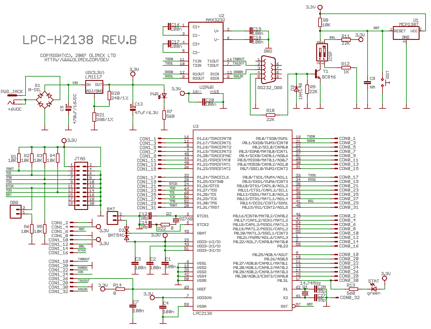
Excuse my ignorance my fellow engineer!! I think I understand what you mean by "connected wrongly… well here is an attempt of me(following the tutorial by sparkfun) to fix my mistake…

Well, I am just wondering… I have seen like 5 schematics and all of them have VREF connected to the power supply… and about the same for VBAT… also, are these(the pins that you suggested me to connect to JTAG aren’t the only ones I see on other schematics) the only ones I need to connect to jtag to program the processor properly? Do I need a reset circuit(rst is connected to jtag though)? Why are the jtag pull ups resistors used in the schematics I see while in the jtag application note there are no pull ups used(It mentions though that the resistors should be used if the distance between the core and the jtag is bigger than 5cm and it isn’t in most of the boards.), all the boards I saw were from Olimex, micro4you and some boards from the lpc2000 family, the lpc2000 yahoo group files and also some others that I came up googling

http://f1.grp.yahoofs.com/v1/IHFOTTbM5H … s8900a.pdf

According to the link above, the RTCK and TCK pins of jtag are pulled down to gnd.

According to this http://www.olimex.com/dev/pdf/arm-jtag.pdf , the RTCK and TCK should not be pulled down to GND.

The same happens here http://www.olimex.com/dev/pdf/ARM/LPC/L … ematic.pdf

Here http://www.olimex.com/dev/pdf/ARM/LPC/LPC-P2138.pdf

Here http://www.olimex.com/dev/images/ARM/LP … -B-SCH.gif

but not here http://f1.grp.yahoofs.com/v1/IHFOTRckij … LPC-L1.pdf

What shall I do? Also will I be needing a dbg jumper?

I got my answer while searching on google, and if still someone came here looking for an answer to my question above here it is…

The pull-down resistors are to keep the logic level going into the gate at ground until the button is pushed.

IC's are VERYY sensitive to ESD (Electrostatic) and if you leave the inputs 'floating' (not conected) they will pick up signals from a range of things...

and you dont tie the input straight to ground to keep it at logic 0 because when when you press the button you will make a short circuit.
The resistor acts as a load.

It is a high value resistor to heavily limit current, but the IC will still pick up the logic levels.

You can change the resistor value to 10K if you want.