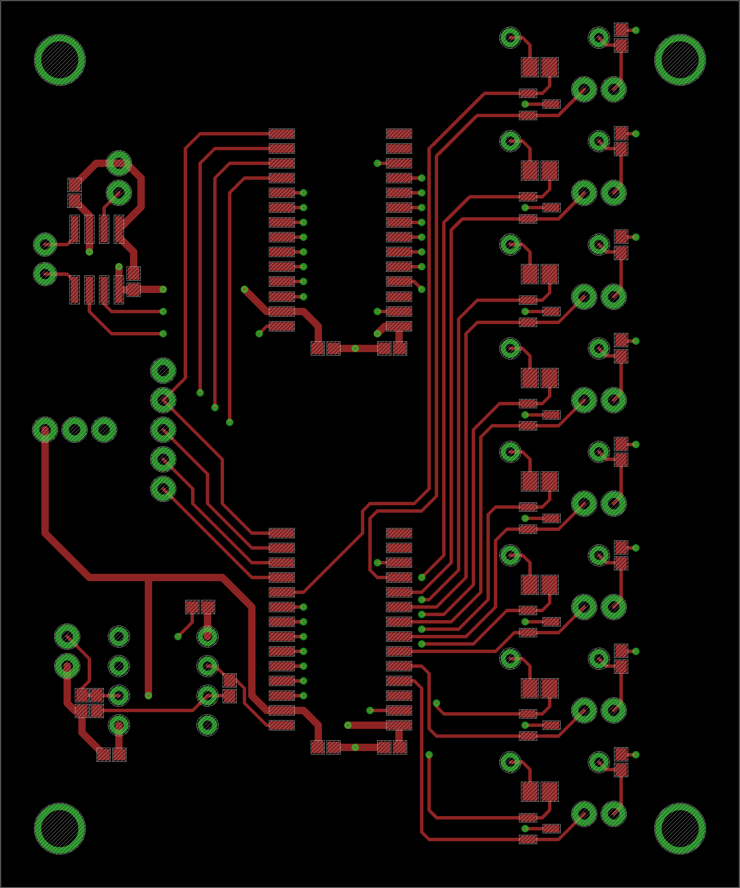
I’d appreciate it if I could get a check on a PCB design. While I have some small previous PCB design experience, I’ve not done a multilayer board before, or one with such dense traces, so I want to make sure I’m avoiding any major mistakes.
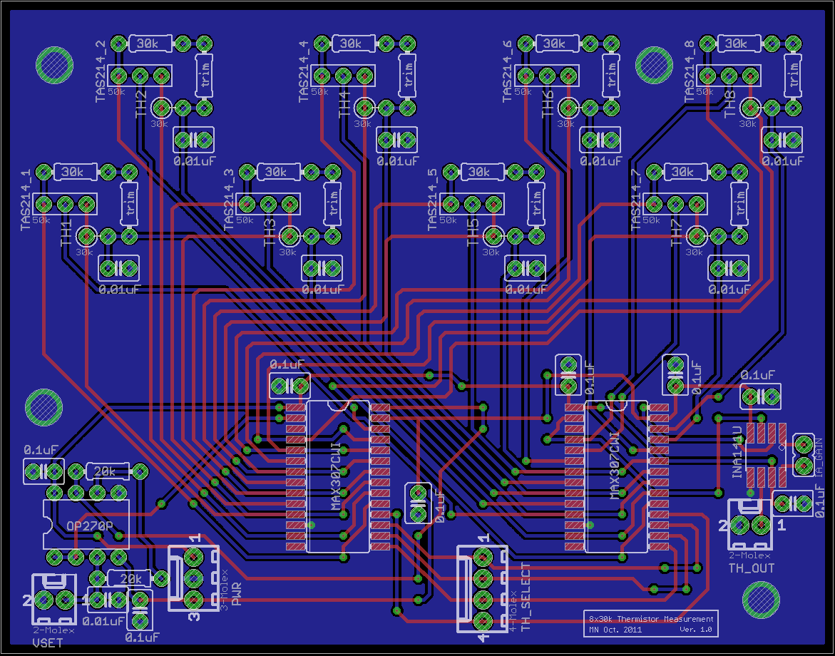
This project is a thermistor measurement board using Wheatstone bridges, with the ADC elsewhere (via lower-right molex). The 3-pin devices are precision 50k resistor pair nets, and I have a 30k + trim resistor with the 30k thermistor. I’m using an analog mux to power and read one thermistor at a time in order to minimize self-heating. Power is +/-15V, with a DAC line (lower-left molex) to allow variable bridge voltages (more for higher precision, less for higher range). Edit: updated with silkscreen (accidentally included origin layer as well).
Some potential issues I can think of are:
- Edit: added grounded mounting holes (Note: these forums really need to enable tags!)
- The via clearance in the buses seems somewhat small - does it look ok?
- Are the trace clearances in the bus ok?
- I'm routing power through some device pins, not via a star bus. I think this should be ok, as I'm not dealing with any fast signals.
- I don't have a ground pin on the mux selection plug - I wanted to avoid using a 5-pin molex, and it will be grounded at the case. I can add one if it's particularly important, but these are digital signals that will not switch quickly.
- The ground plane doesn't quite go between any of the device pins. I don't think this is a problem, and none of the pour areas are isolated, but I could reduce pour clearance or pad size if needed.
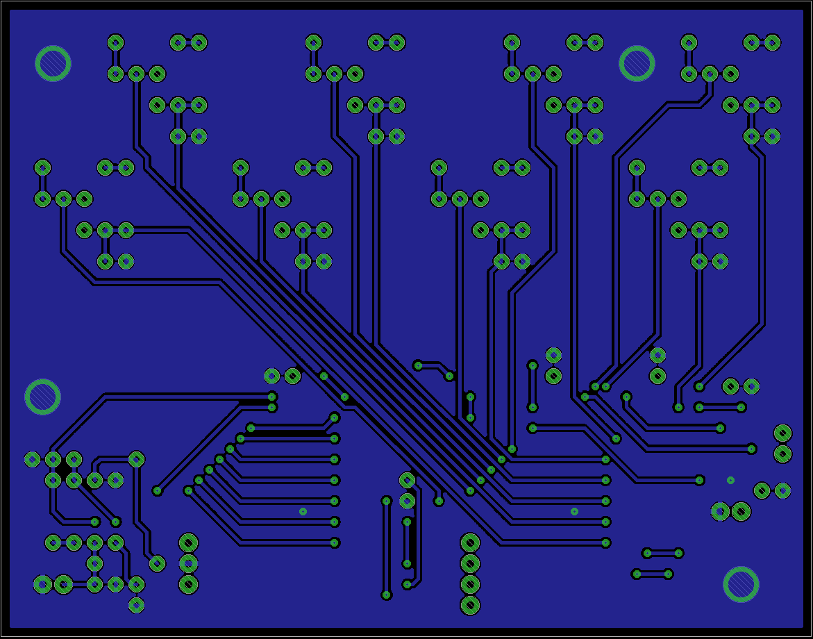
Images as links because they’re 1200px across, and may break board formatting:
First off, for someone who has not done a multilayer board or anything this dense before, this is a top effort, nice work.
To answer some of your questions:
- *The via clearance in the buses seems somewhat small - does it look ok?*
These are fine. I put the board through a 10mil clearance DRC check and it passed fine, most board houses will go 6/6mil or 8/8mil trace/space these days.
- *Are the trace clearances in the bus ok?*
Most of the bus lines have what looks like around 16mil clearance which is plenty.
- *I'm routing power through some device pins, not via a star bus. I think this should be ok, as I'm not dealing with any fast signals.*
You’re right, it’s not ideal, but since it’s only DC and you have de-coupling caps on the ICs it’s good enough.
- *I don't have a ground pin on the mux selection plug - I wanted to avoid using a 5-pin molex, and it will be grounded at the case. I can add one if it's particularly important, but these are digital signals that will not switch quickly.*
This depends on where these digital signals are coming from. Personally I would put a ground pin on the plug to avoid nasty things like ground loops.
- *The ground plane doesn't quite go between any of the device pins. I don't think this is a problem, and none of the pour areas are isolated, but I could reduce pour clearance or pad size if needed.*
This isn’t really a problem. If you want to fix it, simply change the width of the polygon line to something like 8mils.
A few observations, but no show stoppers:
- Your traces all seem to be 16mil wide. Your board is fairly large so you could make some of the power traces thicker. For reference, on a standard PCB allowing 10°C temperature rise, an external 16mil trace will carry ~1.2A of current.
- It's just an aesthetics thing, but I would try and get the 4 mounting holes in the corners, and then radius the corners of the board to make it looks nice and professional.
- It's not clear what layers you are using for your silkscreen, I always use separate layers for silkscreen so I can control what is on them, but that's a personal choice.
- I can't see a single 90° trace corner on the entire board, which is excellent!
- If I was to have laid out this board, I would have rotated the two MAX307 ICs 90° CW. This would tidy up much of your buses routing.
- Your board dimension is are 3.887008x3.049606 inches. This doesn't matter at all but I would at least align the dimension lines to the grid.
Really, I am just nit-picking in anything I can (which is what us engineers do). The board looks great and is an excellent first multi-layer board.
Place them in the corners about 5-6mm away from the edges, all in line with rounded off numbers between them I.E. 100mm not 99.32
Placing the mounting holes in the corner will ensure that when screwing the terminals for the VSET and PWR molex - the board is supported otherwise it will flex the board and can damage the joints.
I would also ensure that all terminal blocks are outward facing
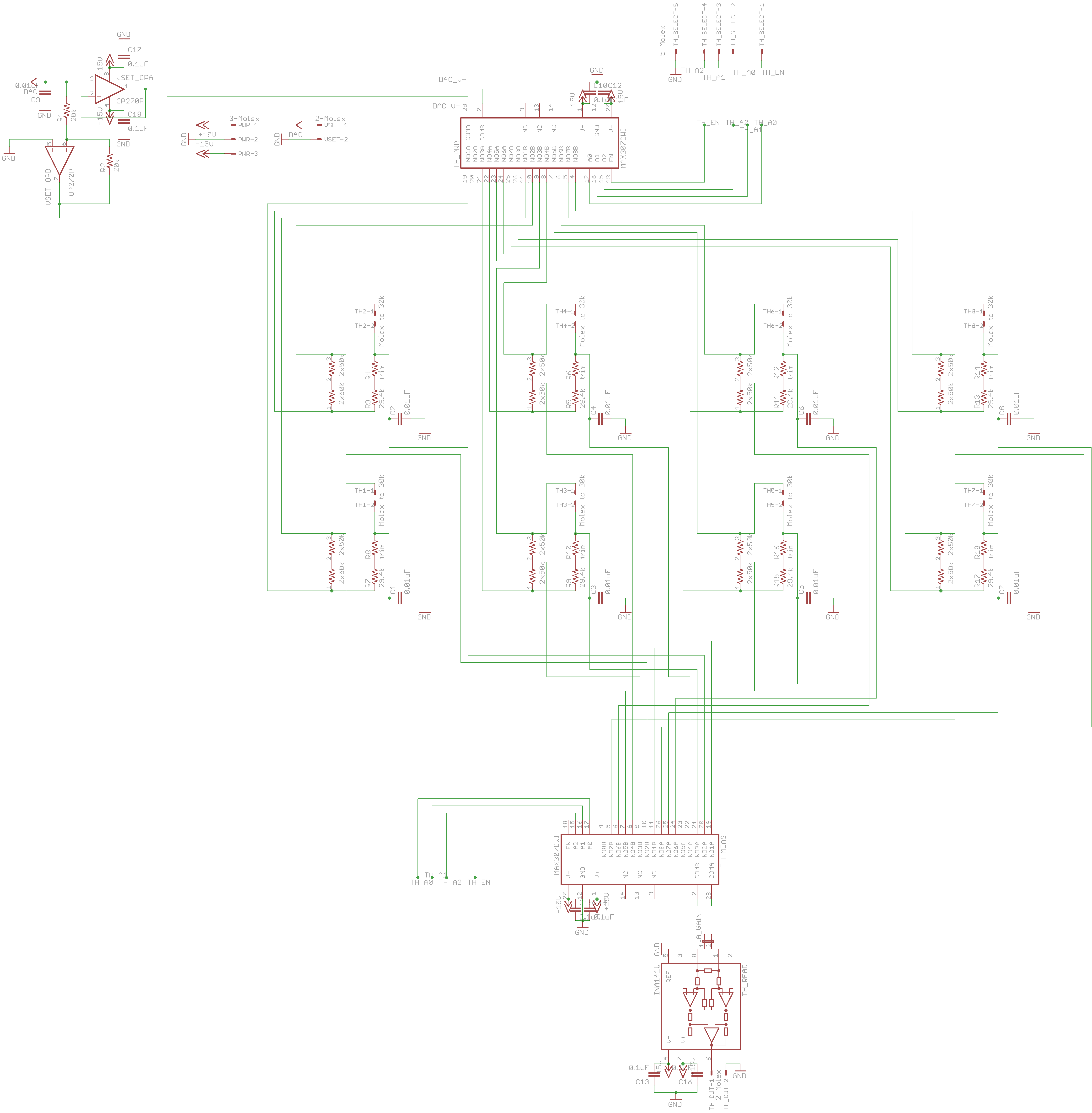
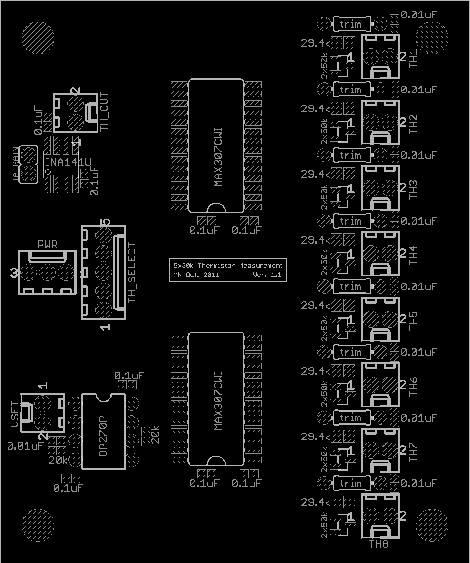
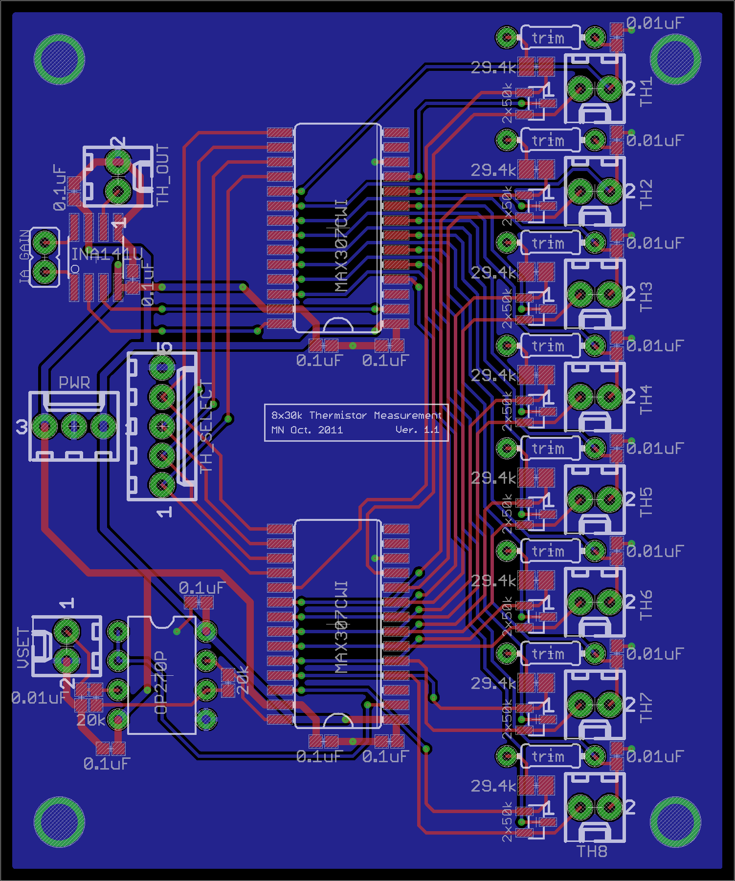
Thanks for all the helpful suggestions! I had some problems with the Sparkfun forum, so couldn’t post earlier, but I redesigned the board over the weekend.
Using several of the suggestions (especially rotating the MAX307s - not sure why I didn’t before), and with SMT parts where it was possible (I found a nice 100k 0.035% voltage divider in a SOT23 package), I shrunk the board to 2.5x3", and put it in a more linear layout. I also added a semi-star 24mil power bus. I did have to reduce the vias to an 8mil drill, 8mil pad to have 8mil clearances, and I reduced the signal traces to 10mil. I imagine this should be fine, the signal lines shouldn’t be carrying more than 1mA at absolute worst case. I plan to have the board manufactured by [PCBexpress, and they go down to 6mils, with an 8mil minimum drill. Also, I changed the thermistor connections to molex connectors - it will be more convenient than soldering the leads directly.
Here’s the new board:
- [[The full board](http://jila1.nickersonm.com/thermmeas_all_1.1.png)
I’ll be double-checking the power molex polarity and SMT land patterns before finalizing it, but other than that I think it’s in it’s final state. I’d appreciate a quick review of it in case I missed something, though.
Nice work! I’m glad you redesigned the board, it looks much more symmetrical and professional now.
A few things:
- All the vias seem to be 8mil. I wouldn't use the minimum drill unless you have to, especially on the power traces which I would bump up to 20mil or thereabouts. Signals are fine at 8mil so 10mil is prefect.
- Your mounting holes are grounded. Some people prefer it but make sure you are aware they are grounded, possibly with a small ground symbol near them. You can replace them with a simple "hole" for ungrounded holes. I would also round the corners of the board (using "miter") but that's simply for aesthetics.
- The footprints for the trimmer resistors, are they correct?
- Silkscreen - I would edit the molex silkscreen so those numbers are either not visible or positioned more optimally. The connectors are polarised so pin number shouldn't need to be indicated. (The "1" on TH_OUT for example covers a pad. Make sure PCBExpress will clip this so it doesn't get printed over your pads, which makes soldering less fun.)
The only other thing that stands out are the SOT23 resistor dividers. These are usually quite expensive (compared to normal resistors), although their precision is very good. As long as your aware of the cost and you have determined that you need 0.035% tolerance then it’s all fine.
Make sure to post back with pictures once you have built the board!
Thank you! I am trying to make it as neat as I can. I did just notice that the bus on the bottom copper was needlessly crooked, so I straightened that out.
I used the minimum drill size for vias because the next larger is 16 mils, which causes clearance problems with the vias. I bumped up the power vias to 20mil, though. The mounting holes are also intentionally grounded vias, yeah.
While the footprint for the trimmer resistors would probably have worked, it was a bit crowded, so I increased it to the next size up, since I have the spare space. I also took the time to remove the molex pin numbering, thanks.
Regarding the resistor dividers: yeah, they’re slightly expensive ($2 each), but less than the SIPs I was originally budgeting for. Reducing to 0.1% tolerance doesn’t really save much, either, and I wouldn’t want to go much below that. Having a high precision match is useful to avoid worrying about room temperature drift affecting my calibration and such.
I’ll be sending my order in tomorrow morning, so I’ll probably have the board by early next week to show off :).
Thanks again for everyone’s help, it’s been very useful.
The PCBs came in on Monday, and look good. I just soldered the SMT parts on one of them today (paste syringe + IR oven), and it surprised me how easy it was, not having worked with either solder paste or SMT parts before. The process is a lot more forgiving than I expected - and the 0603 parts are a lot smaller in person!
Thanks for everyone’s help. I’ll post some pictures this evening when I can get to my camera.
nickersonm
Edit: Images of the unpopulated and populated board! The trim resistors aren’t in yet, since they will depend on the value of my individual thermistors.