Hi everyone,I’m working with the LTC3588 for a piezoelectric harvesting project. I am encountering a strange issue where I cannot get any output voltage across Vcc and GND.
Setup: Source: 4 Piezoelectric disks in series.
Input: Currently using an external bridge rectifier connected directly to Vin and GND (if I use the on-board PZ1/PZ2 pins, the input capacitor doesn’t charge at all!
.Capacitance: 100 micro Farad on V_in, on Vin and GND.
D1 tied to V_in, D0 tied to GND (for 3.3V mode). EN tied to V_in
The Problem: my Vin capacitor charges quickly and stabilizes at 8V, which is well above the 5.05V UVLO threshold for the 3.3V setting. However, Vcc stays at 0V. If the internal bridge rectifier is blown, would that also prevent the buck converter from regulating even if V_in is powered externally? Or am I missing a specific “cold start” requirement for the EN pin? Any advice on troubleshooting the buck converter stage would be greatly appreciated!
There’s a few things that stand out to me
100uf seems too high, I think it wants 1-10
Tying D1 to Vin violates the threshold [from datasheet’s Absolute Maximum Ratings, the voltage on D0 and D1 must not exceed the lesser of (VIN2 + 0.3V) or 6.0V]; tie it to Vin2 instead (there’s a jumper for this purpose)
What is Vin2 reading while Vin1 is 8v?
Thank you for the clarification — that helps.
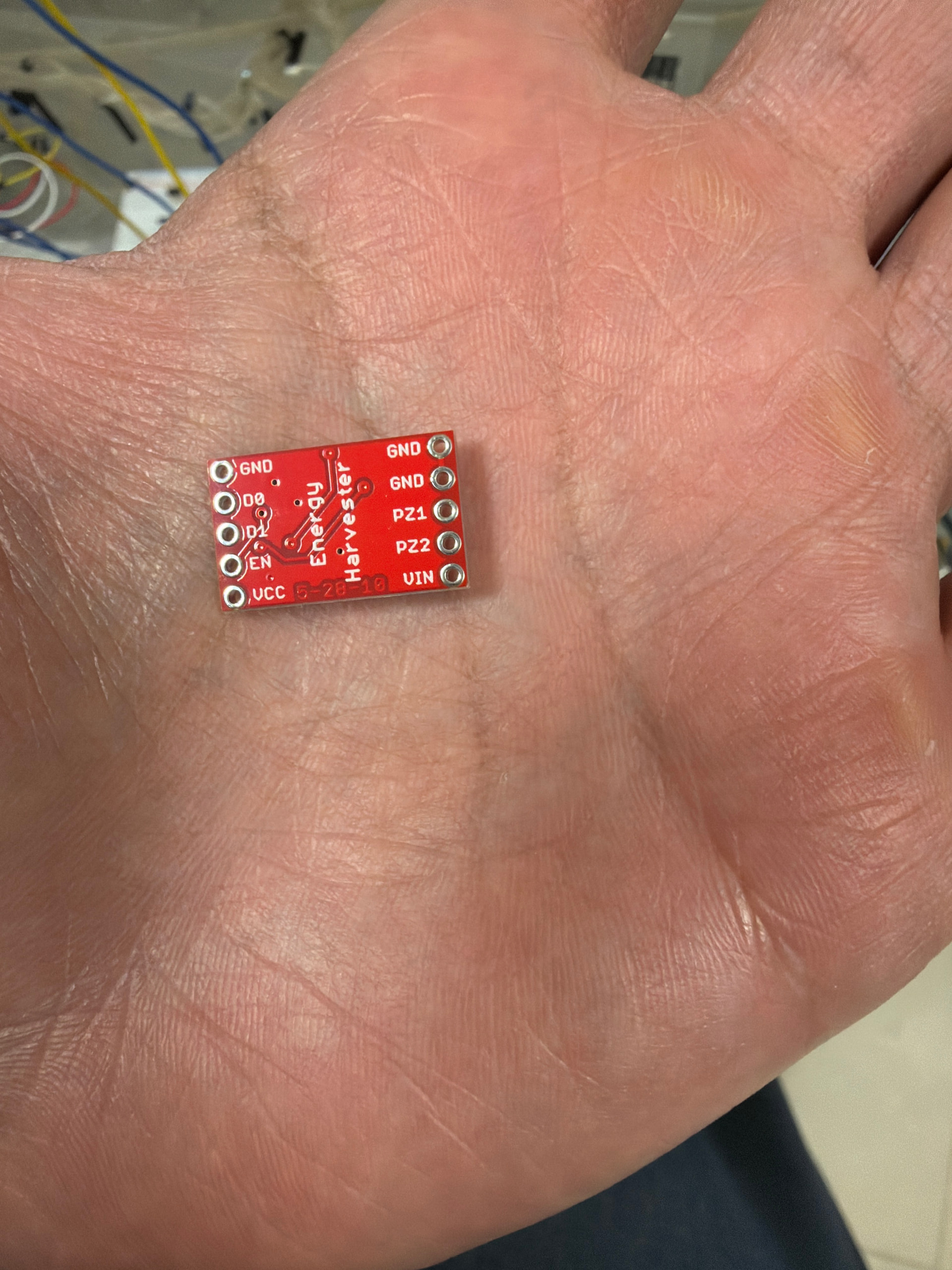
On the SparkFun Energy Harvester breakout I do not see an exposed pin or labeled test point for VIN2 on either side of the PCB (only VIN, PZ1, PZ2, VCC, EN, D0, D1, and GND are accessible). I’ve attached photos of the board for reference. Could you please point me to the exact pad or jumper location where VIN2 can be probed on this revision of the board?
I am new to the LTC chip. Could you please guide me for a basic troubleshooting that give 3.3 v across Vcc and GND! to see if my chip is working fine or broken!
Also my chip doesn’t work when I connect the piezo wires directly to pz1 and pz2 that is why I had to build my own full rectifier with 4 diodes, then feed to Vin and GND.
I tried to replace the capacitor from 100 micro to 4.7 microFarad, yet I got similar results. I even removed all the wires from EN, D0, and D1. The capacitor still charges quickly to around 6~7 volt but the Vcc is still 0!
So what is the correct wiring incase if I order a new one. Which I leave EN, D0, and D1 untouched! Leave it without any jumper wires? Or I should hook EN to Vin?
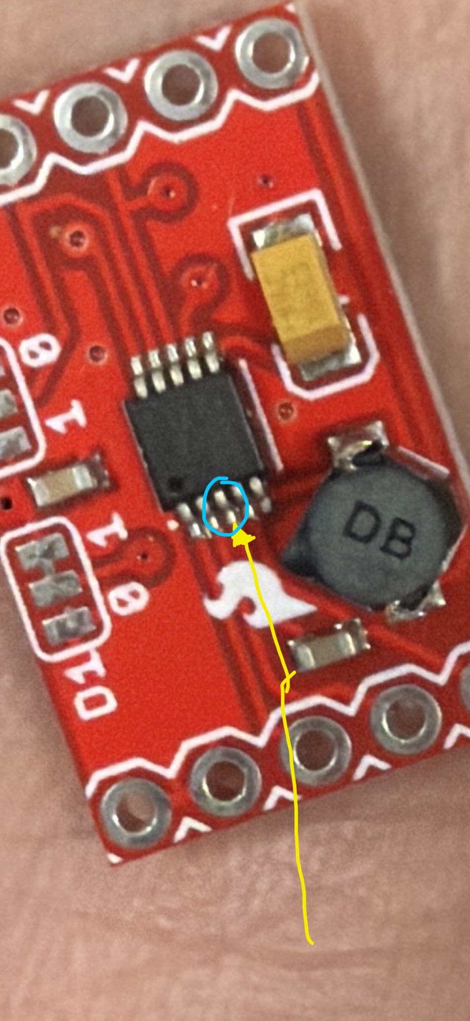
It’s a jumper pad labeled on the front…but after seeing the photos I believe the main issue is that things weren’t soldered…you’ll want to solder pins before testing
Chip is very unlikely to be broken or you wouldn’t see vout
- Should I solder these pins in the middle? 10 pins in total?
aside from that? Kindly please answer my question regarding proper wiring in order to get 3.3 v at the output (Vcc and GND)
- Should I leave EN, D0, D1 untouched without any jumper wires to get 3.3v at the output?
No, I meant the PTH holes on both sides of the board edges
It should be pre-configured for 3.3v if you supply a steady voltage above the threshold…but you’ll need to solder pins to be sure the power is actually propagating correctly