If you are making this at home, you may have to worry about narrow traces. If you are going to use a board house, then check its design rules. Most places can handle traces and spaces down to 8 mil. Some can do 6 mil.
Regarding your board - traces should intersect only at 90 degrees, not something smaller like 45 degrees. BTW, 90 degree corners are OK, though 45 degree corners look better.](http://img.radiokot.ru/files/106011/medium/n1o0d4l4o.png)
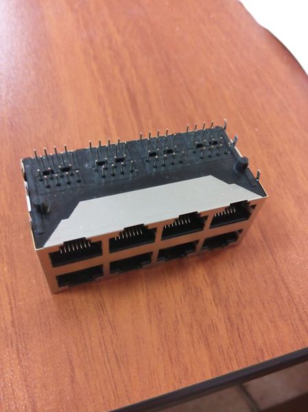 <LINK_TEXT text=“http://img.radiokot.ru/files/106011/thu … p6kdur.jpg”>http://img.radiokot.ru/files/106011/thumbnail/n0gp6kdur.jpg</LINK_TEXT>
 <LINK_TEXT text=“http://img.radiokot.ru/files/106011/thu … jejfch.png”>http://img.radiokot.ru/files/106011/thumbnail/n0gjejfch.png</LINK_TEXT>
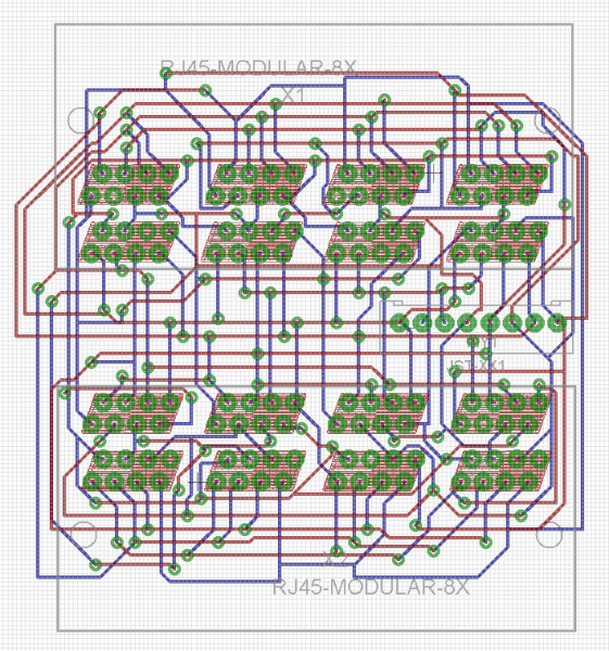 <LINK_TEXT text=“http://img.radiokot.ru/files/106011/thu … jf2g6r.png”>http://img.radiokot.ru/files/106011/thumbnail/n0gjf2g6r.png</LINK_TEXT>
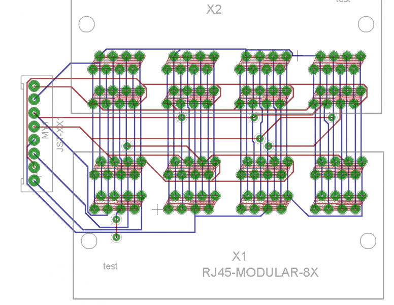 <LINK_TEXT text=“http://img.radiokot.ru/files/106011/thu … 0d4l4o.png”>http://img.radiokot.ru/files/106011/thumbnail/n1o0d4l4o.png</LINK_TEXT>